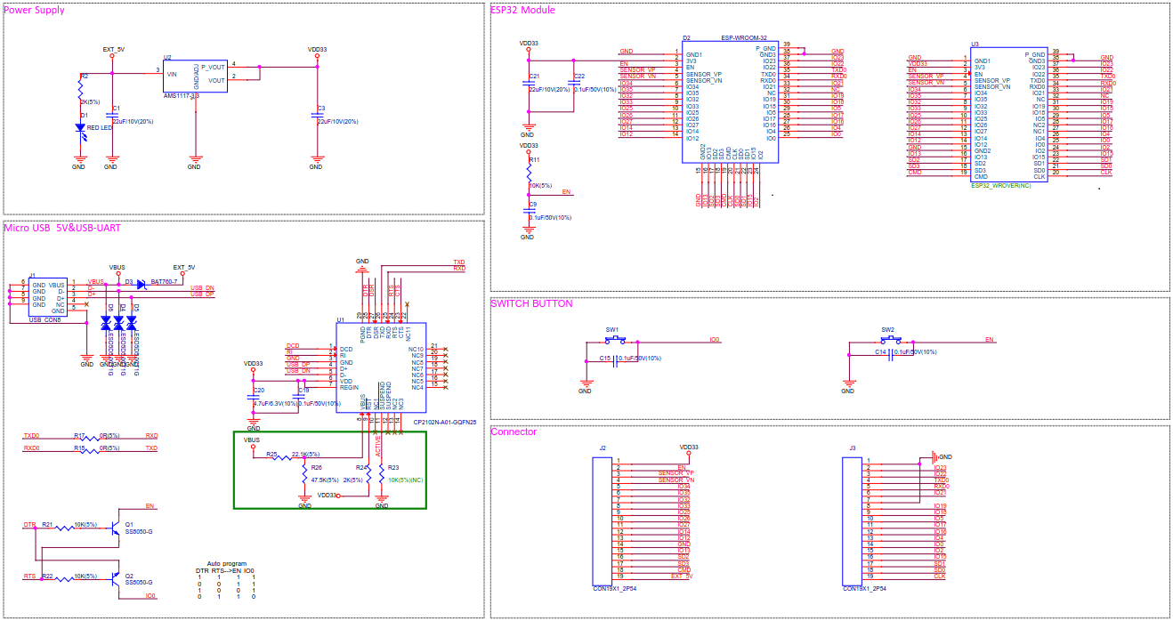
Overview

As a beginner of learning circuit boards, it was difficult for me to understand the functionality of each component of the ESP32 devkit board schematic. So, I have analyzed the ESP32-DevKitC V4 board and written a summary this time. The schematic itself and the starting guide from ESPRESSIF helped my understanding a lot.
The following another schematic and websites were also helpful to stretch my understanding.
- DOIT ESP32 DEVKIT V1 schematic
- ESP32-WROOM-32D開発ボードの仕様・機能
- ESP32 Pinout Reference: A Comprehensive Guide
- Getting Started with the ESP32 Development Board
You can buy the ESP32-DevKitC V4 board from here.
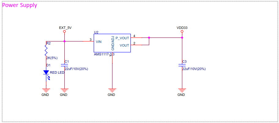
Power Supply
AMB1117-3.3 is a component for regulating the voltage to $3.3 \, \mathrm{V}$. A capacitor of $22 \, \mu \mathrm{F}$ is recommended for stable operation in the datasheet. An LED light lets us know current is coming through from the power supply. Good to put a resistor to protect the LED from large current flow.
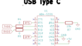
Micro USB 5V & USB-UART
This is the overview of the schematic related to the USB connection.
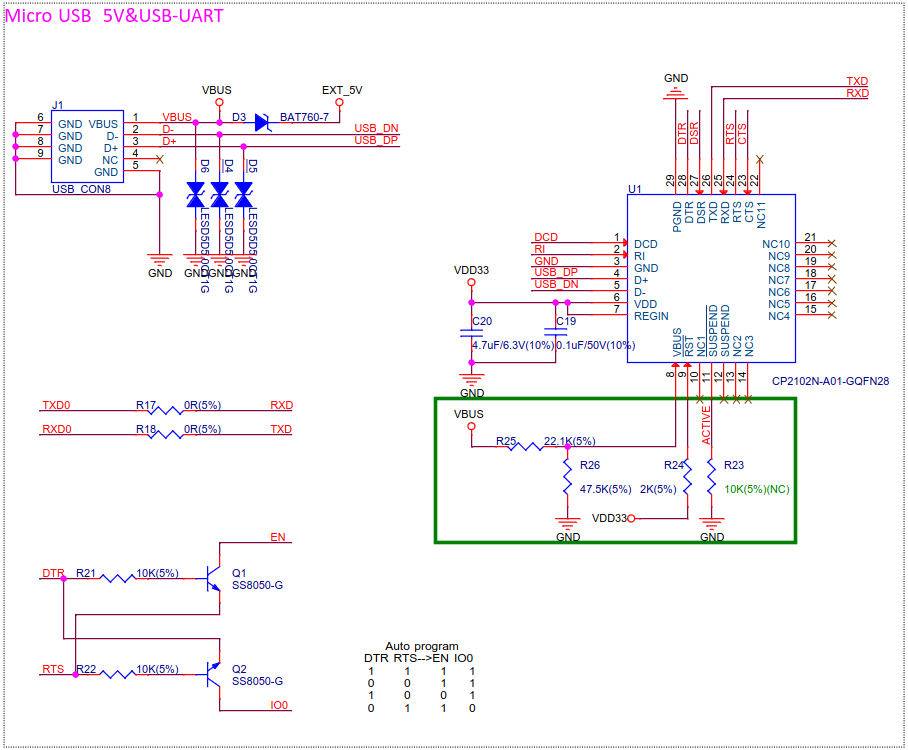
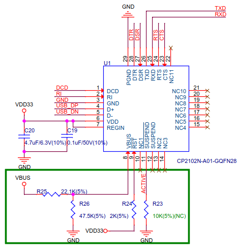
CP2102N chip functions as a USB-to-UART bridge controller. The datasheet on the chip can be found here. The connection between the chip and the other components is shown below.
Since this is a complex circuit, I will explain the circuit diagram in several parts.
Auto program: DTR and RTS
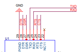
What DTR, DSR, RTS, and CTS stand for is explained here in detail (the difference between DTR/DSR and RTS/CTS are also clearly described). Briefly speaking, those can be summarized below.
| DTR | Data Terminal Ready | The host computer is ready to communicate |
| DSR | Data Set Ready | The end device is ready to communicate |
| RTS | Request To Send | The host computer is ready to send data |
| CTS | Clear To Send | The end device is ready to receive data |
The following websites explain the meaning of the circuit above.
- Explain why the NodeMCU auto-program circuit would be useful
- ESP8266にDTRとRTSで自動書き込みをする
- Having problem in understanding how DTR and RTS pins are working here in the given schematics?
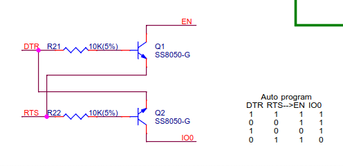
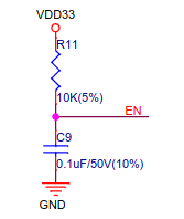
Referring to the official documentation, we need to make IO0 low, and then EN low to put the chip into firmware download mode. This is done automatically by the auto program circuit.
EN and IO0 are both high when DTR and RTS are both high or both low since they have pull-up resistors (IO0 has an internal pull-up: you can find the information on ESP32 Datasheet 2.4 Strapping Pins).
Furthermore, when DTR is high and RTS is low, current comes through from Q1 BJT’s collector to the emitter, as a result, EN becomes low. In this case, current does not flow on Q2 BJT since it operates in the cutoff region, and IO0 remains high.
The same applies in the case that DTR is low and RTS is high.
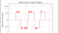
The following diagram shows DTR, RTS, EN, and IO0 pin voltage (High / Low), respectively.
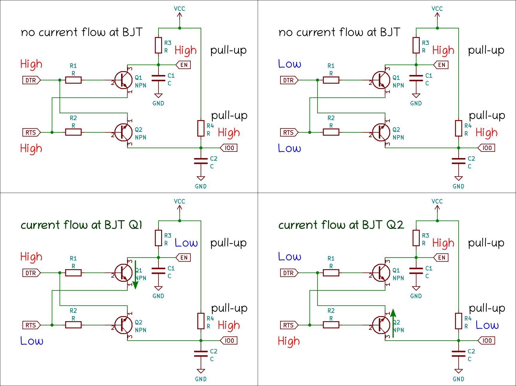
This youtube video was helpful to gain a basic understanding of the bipolar junction transistors.
DTR is asserted by the computer, and then it asserts RTS when establishing communication (ref1, ref2). This achieves IO0 low, and then EN low.
Data communication: TX and RX

TX / RX of CP2102N and RX / TX of ESP32 are connected for data communication. TX is for transmitting data and RX is for receiving data. RX pin of a device is connected to TX pin of the other one.
These sites teach us a lot about UART communication.
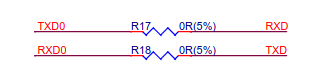
They put $0 \, \Omega$ resistors. The purpose of putting them is summarized here in detail. The resistors are for debugging purposes; we can install another value resistor after fixing the board design.
Power control: RSTb, VDD, and REGIN
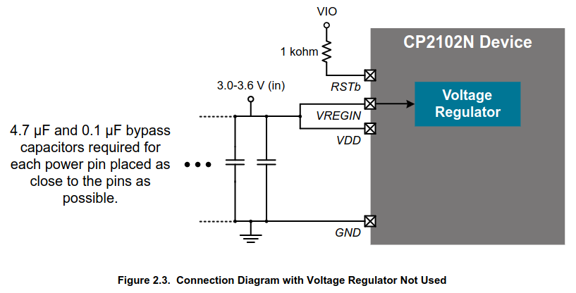
A pull-up resistor is connected to RSTb in both the example circuit of the CP2102 datasheet and the ESP32 devkit board.
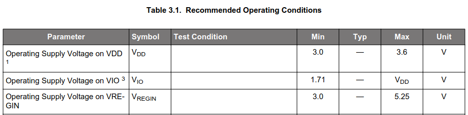
CP2102N of the devkit board uses 3V3 for the power control. This suffices the recommended operating condition.
$4.7 \, \mu \mathrm{F}$ and $0.1 \, \mu \mathrm{F}$ capacitors were chosen for voltage surge filtering. Using two capacitors is common in circuit design as described below.
Typically people use a pair of caps on a supply line where the low value one is the high frequency noise filter while the larger one (in this case the 4.7uF) is the “bulk” capacitor that acts as a little battery to help smooth out voltage drops locally at that pin..
https://www.reddit.com/r/AskElectronics/comments/13w0qou/does_anyone_know_what_the_purpose_of_the_1uf_47uf/
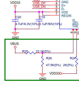
USB connector: D+, D-, and VBUS
The USB cable type used for ESP32-DevKitC is USB Micro B. This website gives us insight into various USB cable types.
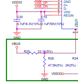
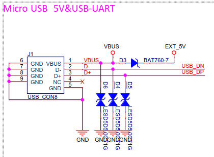
The devkit board has one Schottky diode BAT760-7 and three transient voltage suppressors LESD5D5.0CT1G.
The purpose of BAT760-7 is discussed here. One of the authors concludes that the diode D3 is added to protect the VBUS in the case that external 5V is connected through EXT_5V.
D4, D5, and D6 protect the circuit from ESD (Electrostatic discharge: a sudden and momentary flow of electric current between two differently-charged objects) and transient voltage events.
The circuit board design aligns with the recommended one from the datasheet.
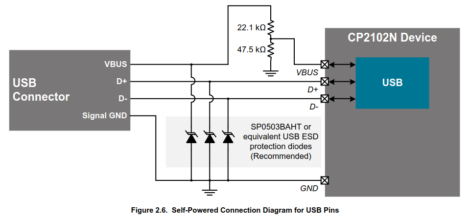
The circuit design in CP2102N datasheet suggests that VBUS PIN of CP2102 should be in the range of VIO$- 0.6 \, \mathrm{V}$ to VIO$+ 2.5 \, \mathrm{V}$, where VIO = VDD equals to $3.3 \, \mathrm{V}$ and USB connector supplies $5 \, \mathrm{V}$ (ref. When we choose $22.1 \, \mathrm{k} \Omega$ and $47.5 \, \mathrm{k} \Omega$ resistors, the divided voltage applied to VBUS is going to be about $3.41 \, \mathrm{V}$ and this satisfies the suggested measure.
Suspend: SUSPENDb
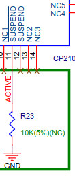
Here is an explanation of the suspend mode.
The CP2102N will enter Suspend mode when Suspend signaling is detected on the bus. On entering Suspend mode, the CP2102N asserts the SUSPEND and SUSPENDb signals.
https://mm.digikey.com/Volume0/opasdata/d220001/medias/docus/322/CP2102N_Rev.1.3_DS.pdf
Putting a pull-down resistor is recommended to avoid floating high in reset mode. This is the reason why the devkit board has a resistor at the pin.
Both SUSPEND and SUSPENDb temporarily float high during a CP2102N reset. If this behavior is undesirable, a strong pull-down (10 kΩ) can be used to ensure SUSPENDb remains low during reset.
https://mm.digikey.com/Volume0/opasdata/d220001/medias/docus/322/CP2102N_Rev.1.3_DS.pdf
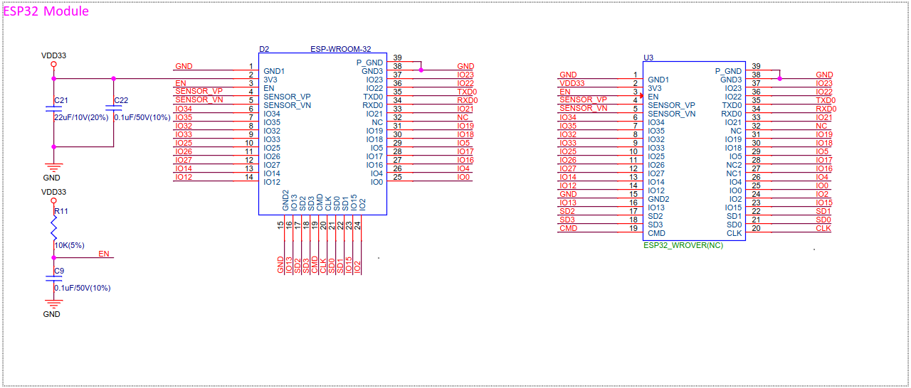
ESP32 Module
A pull-up resistor and capacitors for suppressing ripple and noise are connected to the module. We can choose ESP-WROOM-32 or ESP32_WROVER for the module.
Switch Button
As written in the official guide and this community site, buttons can be used to put the module into the firmware download mode manually. Capacitors are inserted to avoid noise.
Holding down Boot and then pressing EN initiates Firmware Download mode for downloading firmware through the serial port.
ESP32-DevKitC V4 Getting Started Guide
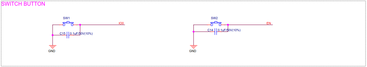
The auto program circuit should enable it to transfer to firmware download mode automatically. Therefore, these buttons are normally not to be used.
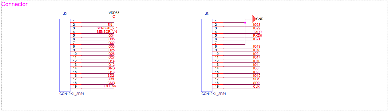
Connector
This is a board used for development purposes, thus it has a lot of pins for debugging.
Summary
What we have learned from the ESP32-DevKitC V4 board is as follows.
- Use AMB1117-3.3 for regulating the voltage to $3.3 \, \mathrm{V}$.
- The auto program circuit uses two BJTs and DTR / RTS lines to determine the voltage of EN and IO0 pins.
- TX and RX lines are for data communication.
- The purpose of $0 \, \mathrm{\Omega}$ resistor is debugging.
- Two capacitors are commonly used for voltage filtering purposes.
- Used ESD protection components for the USB connector.
- Put a strong pull-down resistor to avoid floating high during a reset.
- There are two switch buttons for transferring to the firmware download mode manually.
コメント