I summarized the design of a remote controller with ESP32. My goal is to create the one that controls an omni-wheel robot.
My previous article explains how the official ESP32-DevKitC V4 board is designed.
Here are very good reference videos for drawing PCBs using KiCad (in Japanese).
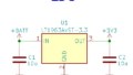
Conceptual design
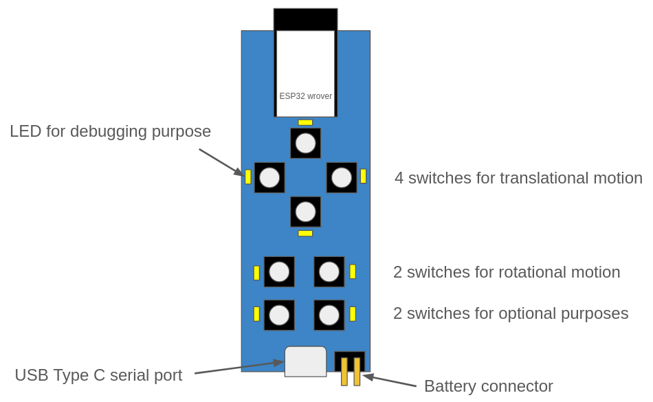
The abstract circuit board design of the remote controller is shown above. It is required to satisfy the following conditions.
- 4 tactile switches for translational motion
- 2 tactile switches for rotational motion
- 2 tactile switches for the optional purposes
- USB Type C port for writing source code and debugging purposes
- Connection to a 3.7V LiPo battery
GPIO PIN allocation
We need at least 8 GPIOs for tactile switches. Referring to the official documentation for PIN allocation, more than 10 PINs can be allocated for GPIO purposes.
This website is also informative for a basic understanding of the tactile switch program.
| PIN | In/Out | Role |
| IO33 | Input | Translational motion (↑ upper direction) |
| IO34 | Input | Translational motion (→ left direction) |
| IO25 | Input | Translational motion (↓ down direction) |
| IO26 | Input | Translational motion (→ right direction) |
| IO27 | Input | Rotational motion (Counter-clockwise direction) |
| IO14 | Input | Rotational motion (Clockwise direction) |
| IO12 | Input | Optional purpose 1 |
| IO13 | Input | Optional purpose 2 |
| IO23 | Output | Debugging purpose LED 1 |
| IO2 | Output | Debugging purpose LED 2 |
Design procedure
To design a PCB, we need to execute the following steps on KiCad. This is just a basic flow.
- Schematic editor
- Draw a schematic
- Annotate schematic
- Electrical rules check
- Assign footprints
- PCB editor
- Draw the PCB design
- Design rules check
Schematic
The overall diagram is here on github. You can find the remote_controller.kicad_sch file there.
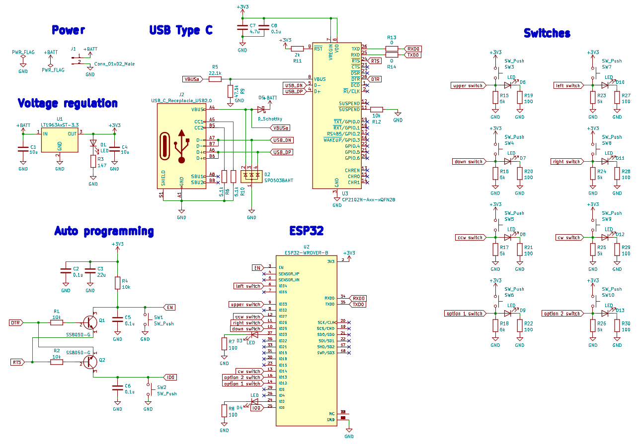
Designed the circuit board referring to the official ESP32-DevKitC V4 board. The role of each part of the official circuit board is documented in this article.
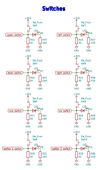
Switches and LEDs
Allocate 8 PINs for switches as follows. A pull-down register should be added to each PIN. As an indication of whether the switch is on / off, add LEDs.
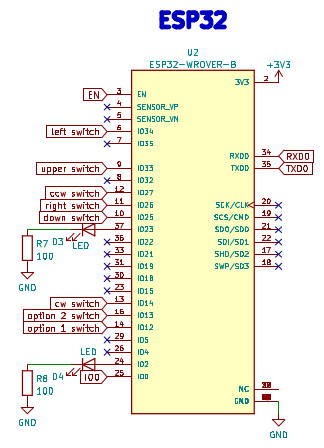
ESP32-WROVER-B
I used the ESP32-WROVER-B module, but its symbol and footprint were not prepared by default on KiCad. Thus, I installed them from this website. The way to install and utilize them is summarized in another article.
Two LEDs for debugging purposes are added on IO2 and IO23.
USB Type C
ESP32-WROVER-B requires USB 2.0 for communication such as writing source code according to this starting guide.
I have confirmed that this module can be used for the communication between ESP32-WROVER-B and the USB type-C cable in this article. Referring to its schematic and the other board’s schematic, wired the components as in the following diagram.
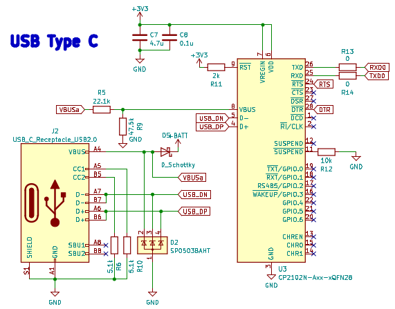
The shield shall be connected to the GND as in the example schematic here. A 5.1kΩ resistor is necessary to be put as a pull-down resistor (citation).
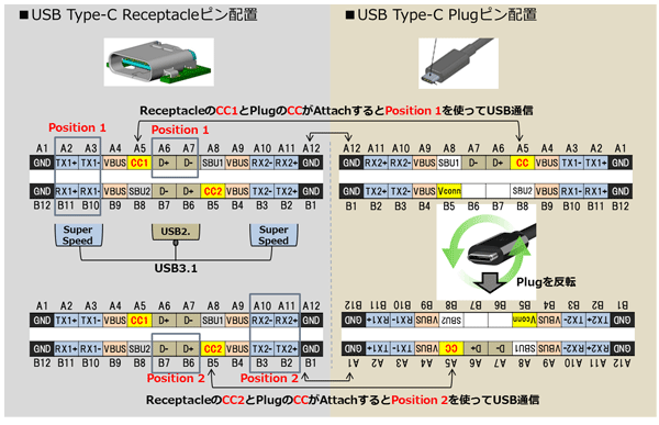
There are duplicate pins since the USB Type C can be inserted upside down (in other words, it is double-sided). The picture below explains this well.
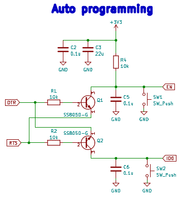
Auto programming
Refer to the basic sample circuit diagram on ESP32-DevKitC V4, and implement auto-programming as follows.
Voltage regulation
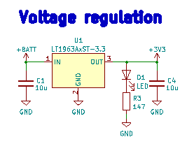
I would like to use a 3.7V LiPo battery to power the remote controller. An LDO (Low DropOut) voltage regulator is chosen to avoid large dropout voltage. The decision process on the LDO LT1963 is explained here in detail. The dropout voltage of AMS1117 (the regulator on ESP32-DevKitC) is around 1.1V; this cannot be used for the mentioned LiPo battery.
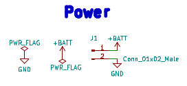
Power
As explained here, we need PWR_FLAG to pass the ERC (electrical rules check). Also, these pins are connected to a connector to the battery.
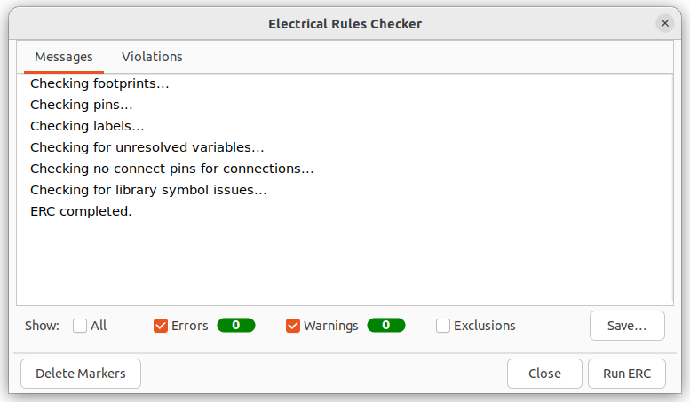
ERC (Electrical Rules Check)
The ERC passes without any issues.
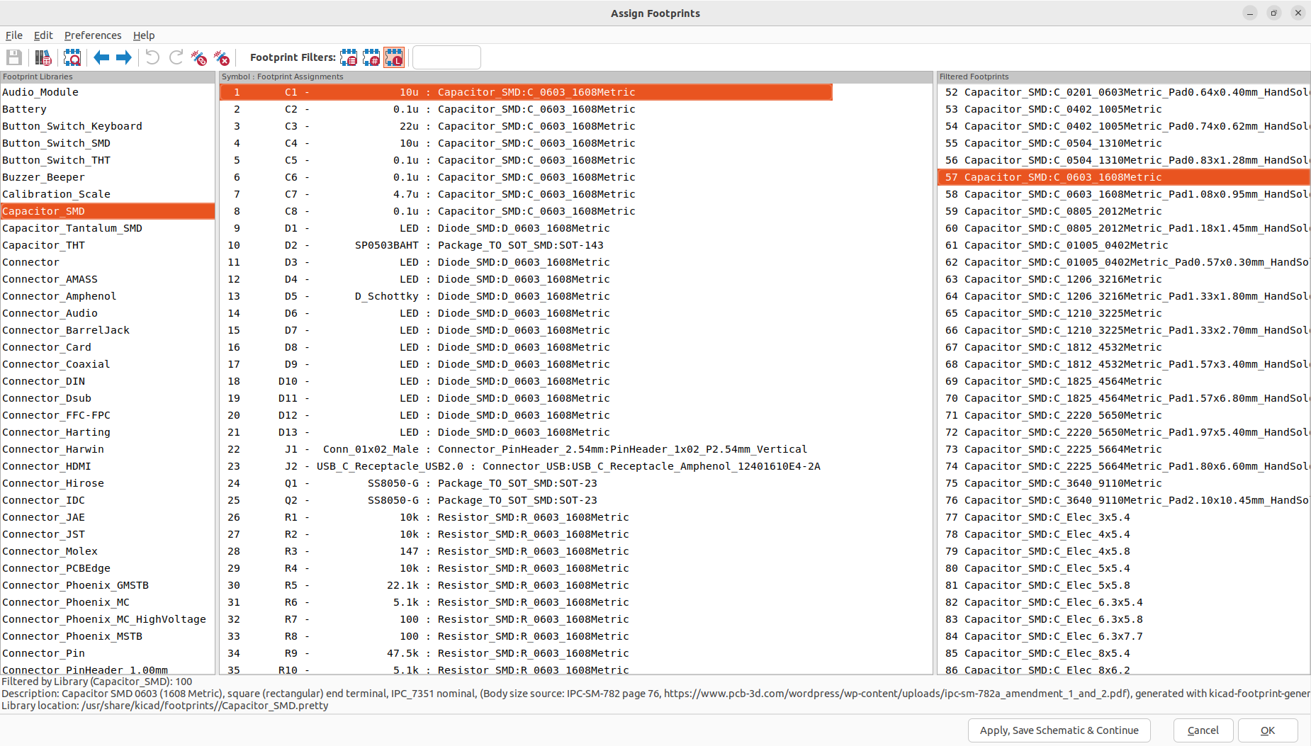
Assign footprints
Assign footprints from the following dialog to prepare for the PCB layout design. Open it by “Tools -> Assign Footprints”.
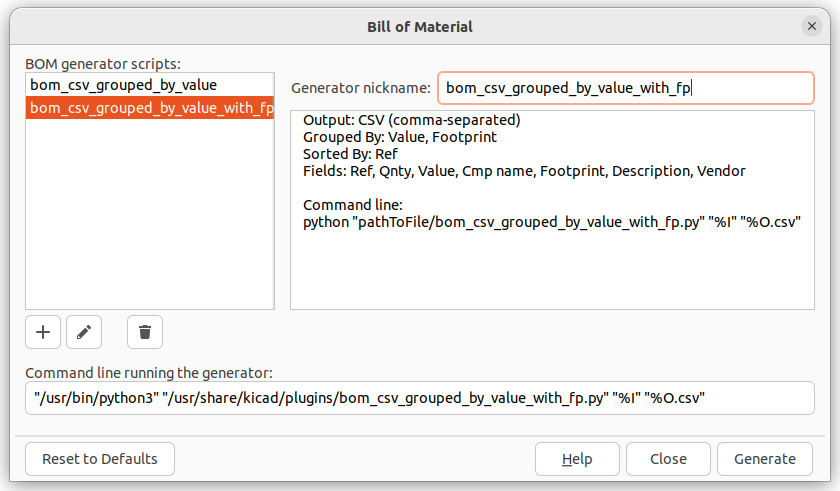
Parts list (BOM file)
This is a screenshot of a BOM (Bill of Materials) file.
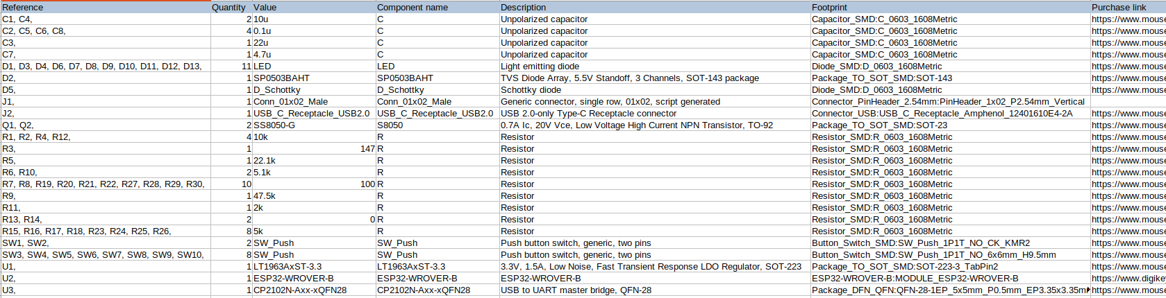
- Chose 0603-inch parts for consistency as for capacitors, diodes, and resistors.
- Except for a battery connector, every component is SMD.
- Except for ESP32-WROVER-B, purchase parts from MOUSER. The one is bought from DigiKey.
The BOM is created by a KiCad script from “Tools -> Generate BOM”.
PCB design
Layout
Both sides of the PCB are shown below.
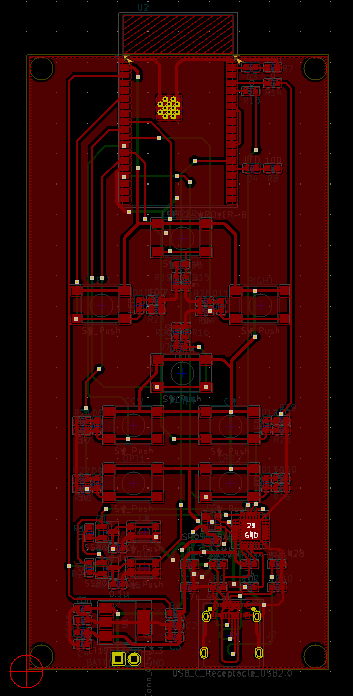
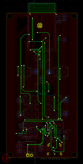
- The height x width of the circuit board is 100mm x 50mm. Added screw holes at each corner.
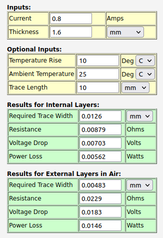
- Assuming that the maximum current is 800mA and the thickness of the PCB is 1.6mm, the width of the line should be wider than 0.00483mm. I have drawn lines with 0.25mm and 0.50mm (power line), those did not have to be so wide… The calculation has been done here.
It has also been observed that the chip draws more than 790 mA at times
Insight Into ESP32 Sleep Modes & Their Power Consumption
- The ground plane is at the front side.
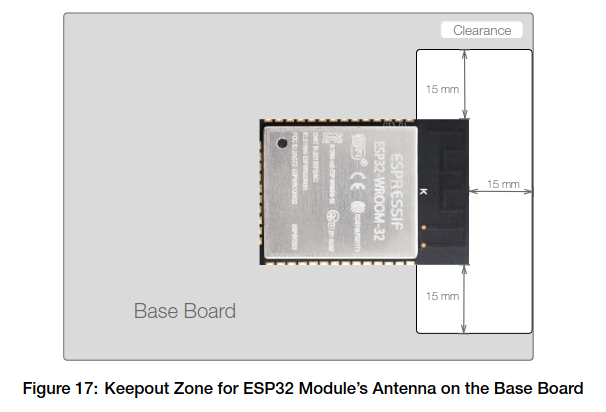
- To minimize interference, the antenna part of the ESP32-WROVER-B module should be placed outside of the base board (reference is here).
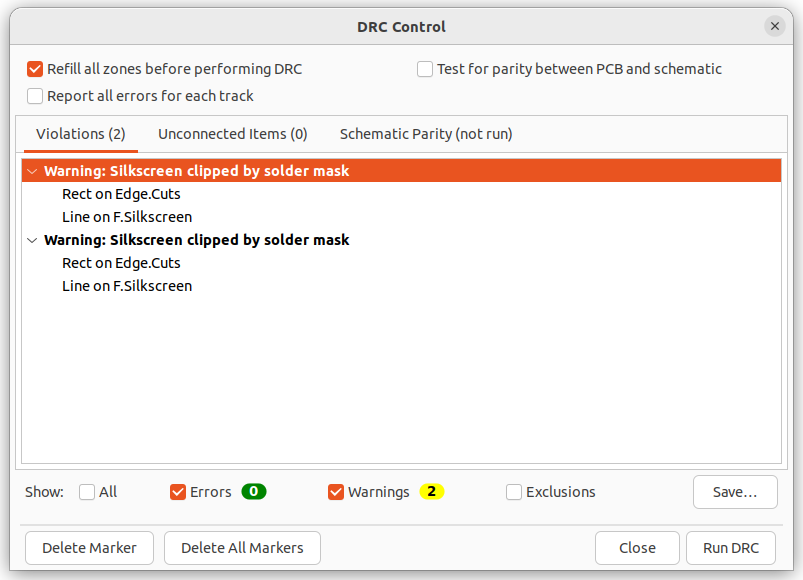
Design rules check
I got two warnings but those were related to the antenna design and we can ignore them since the design is recommended by the ESP32 Hardware Design Guidelines.
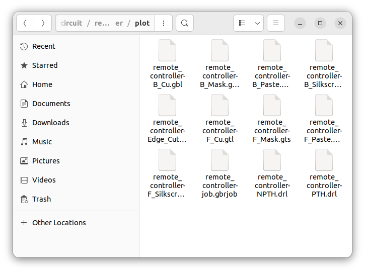
Output gerber data
Click “File -> Plot” and open the following dialog, and click “Plot” and “Generate Drill Files”.
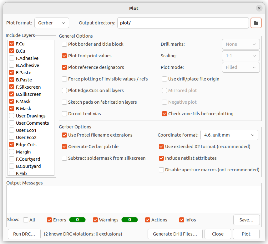
Then, the necessary files to order the PCB are created.
Summary
I summarized the remote controller PCB design. Hope this article should be informative for people who are going to design this kind of circuit board with ESP32.
コメント